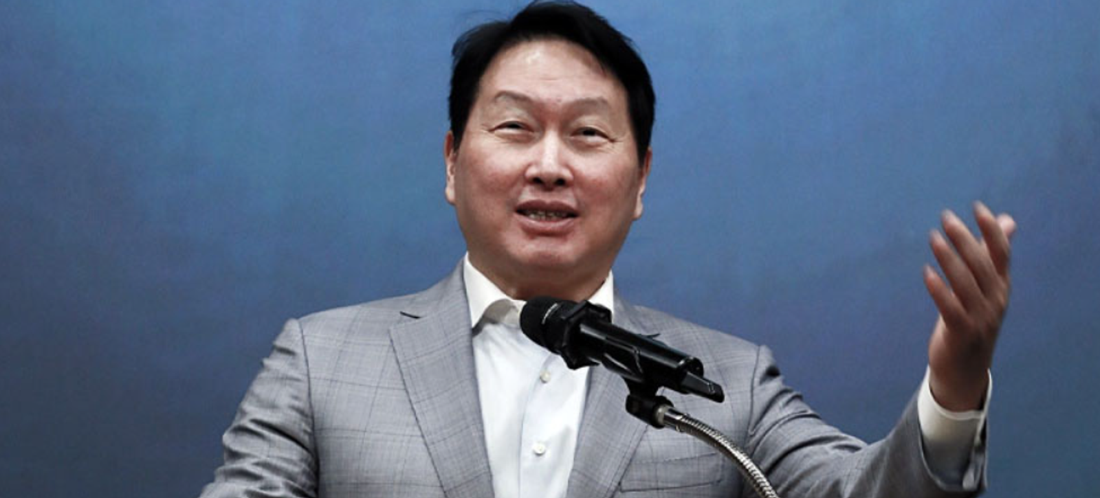
Chey Tae-won, chairman of SK Group, recently visited the proposed site of a new semiconductor fabrication plant — known in the industry as a "fab" — in Gwangju, South Korea's fifth-largest city. He declared his intention to break ground "as quickly as possible," though he acknowledged that delays in securing industrial water and electricity supply could push back the start date. Packed into that single caveat is a telling snapshot of where the global memory chip market stands today.
What is a fab, and why Gwangju?
A fab — short for fabrication facility — is a factory where semiconductor chips are physically manufactured. SK Hynix already operates its main production bases in Icheon, south of Seoul, and Cheongju in North Chungcheong province. Gwangju would become its third domestic site.
The city has long courted a semiconductor cluster, and the central government has pledged support as part of its National Advanced Industry Belt initiative. The economic logic for local authorities is straightforward: a single large-scale fab generates thousands of direct jobs and, when ancillary industries are included, can produce ripple effects worth trillions of won across the regional economy. For Gwangju's municipal government, landing such a project is close to an imperative.
Where does the memory cycle stand?
The memory chip industry is notorious for its boom-and-bust cycles. Rising prices encourage producers to expand capacity; oversupply then collapses prices; investment dries up; shortage returns; prices rise again. The rhythm repeats.
The years 2022 and 2023 brought a brutal downturn. Prices of DRAM and NAND flash — the two principal types of memory chip — fell by more than half, and Samsung Electronics, SK Hynix, and America's Micron all posted losses running to trillions of won. Then, from 2024, the artificial intelligence boom created a powerful new source of demand: high-bandwidth memory, or HBM, the specialised chips that sit alongside AI processors in data-centre servers. The memory market recovered — but only partially.
That qualification matters. HBM remains tight in supply, and prices are holding firm. But conventional DRAM used in smartphones and personal computers, along with NAND flash, remains volatile. By 2025, fresh pressure on NAND prices has emerged from China's push to expand its own chip output and from broader global economic uncertainty. It would be premature to declare that a full upcycle is under way.
The weight of a groundbreaking announcement
Against this backdrop, Chairman Chey's reaffirmation of his intention to build carries two distinct messages.
The first is pre-emptive investment targeted at AI demand. Building a fab from design to mass production typically takes three to five years. Breaking ground now means the plant could be operational in time to capture demand in 2028–2030. AI chips have a voracious appetite for HBM: each Nvidia graphics processing unit is paired with multiple HBM chips, so any producer that fails to expand capacity risks ceding market share. SK Hynix currently holds more than 50% of the global HBM market — a position it can only defend by investing today.
The second message is directed at investors and the government. A single semiconductor factory absorbs tens of trillions of won in capital. An announcement of groundbreaking simultaneously sets in motion financing plans, supply-chain mobilisation, and regulatory approvals. The chairman's personal appearance at the site signals, unmistakably, that this project sits at the very top of the group's priorities.
The infrastructure bottleneck
Semiconductor factories consume prodigious quantities of water and electricity. A large fab can use as much water in a day as a medium-sized city. Samsung Electronics' campus in Pyeongtaek is estimated to account for 1–2% of South Korea's entire national electricity consumption on its own.
Gwangju currently lacks sufficient industrial water infrastructure on the scale required. Expanding the electricity grid entails lengthy negotiations with Korea Electric Power Corporation (KEPCO), as well as planning and construction of new transmission lines. Without these utilities in place, a completed factory cannot operate.
When Chairman Chey said the company would break ground even if water and power supply were delayed, he meant that civil and structural construction would begin immediately, running in parallel with infrastructure work — a strategy to compress the overall timeline by refusing to treat the two processes as sequential.
How to read the next cycle
Many industry analysts place the next peak of the memory upcycle in 2027–2028. Three arguments support this view.
First, investment in AI data centres is likely to keep growing well beyond 2026. Microsoft, Google, Amazon, and Meta have all announced infrastructure spending plans that extend into that period and beyond.
Second, supply constraints will persist for some time. American export controls on advanced semiconductor technology make it extremely difficult for Chinese firms to produce cutting-edge HBM domestically, while expansion by established Korean and American producers is itself constrained by the same infrastructure bottlenecks evident in Gwangju.
Third, a structural adjustment is already under way in NAND flash. Japan's Kioxia and America's Western Digital have both been cutting capacity, gradually working off the supply glut. Many analysts expect NAND prices to enter a recovery phase from the second half of 2026.
Risks, however, are real. A sharper-than-expected global slowdown could cool enthusiasm for AI investment. If China succeeds in developing its own competitive HBM sooner than anticipated, oversupply could return. Escalating trade tensions between Washington and Beijing could also expose Korean chipmakers to further restrictions in the Chinese market.
What to watch
The announcement of a Gwangju fab should not be read merely as a regional development story. It is a declaration by one of the world's leading memory producers that it is confident enough in demand over the next two to four years to commit capital on a massive scale. For anyone tracking the trajectory of the global semiconductor industry, the pace of infrastructure preparation in Gwangju — and the moment the first shovel actually enters the ground — will serve as a reliable indicator of how the memory cycle is truly unfolding.